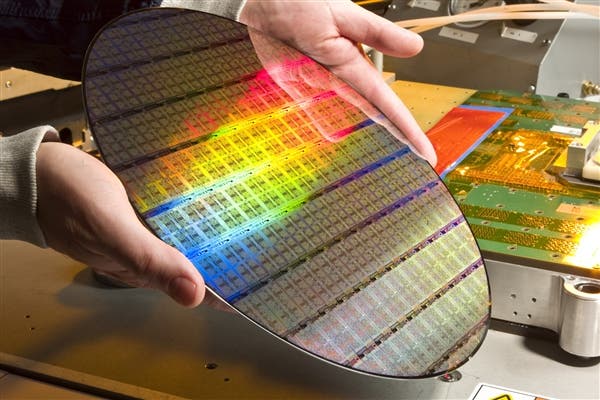
In the semiconductor foundry market, TSMC is the global leader, and the company occupies over 50% of the global market share. It is the first to mass produce the 7nm and other advanced technologies. It is also poised to be the first to mass produce the upcoming 5nm process. However, it appears that Samsung, another semiconductor giant wants to give it a fight for the 3nm process. Next week, Samsung will announce its 3nm process map which would obviously challenge TSMC.

TSMC mass produced the 7nm process ( N7+ ) last year. This year, it is now on the second-generation 7nm process (N7+) which uses EUV lithography. In 2020, it will turn to the 5nm node. The risk trial production will be carried out in the Fab 18 plant, and commercial production will be officially launched in the second quarter of 2020. Next year’s 5nm process is the first generation of 5nm, and there will be an upgraded version of the 5nm (5nm+). It is expected to be in trial production in the first quarter of 2020 and mass production in 2021 .
Samsung announced a series of roadmaps last year, and it is more aggressive than TSMC. It directly entered the era of EUV lithography and has produced a 7nm EUV process chi. It is currently on the 5nm process but is already looking ahead to the 3nm process node


