Samsung completes 8nm 5G RF solution development - see details
SamsungWednesday, 09 June 2021 at 15:37

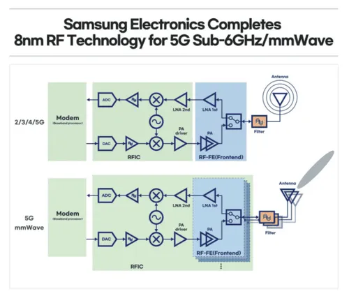
Samsung officially announced that it has successfully completed the development of the latest radiofrequency technology based on the 8nm process. According to Samsung, this advanced process technology will provide a "single-chip solution" for 5G communications. It is specifically designed to support multi-channel and multi-antenna chip designs. Samsung's 8nm 5G RF solution will extend the company's leadership in the 5G semiconductor market from the Sub-6GHz frequency band to millimeter-wave applications.

Samsung's 8nm 5G RF solution is the latest addition to the currently widely used RF-related solutions. Samsung has multiple RF solutions with the 28nm and 14nm processes. Since 2017, Samsung has shipped more than 500 million mobile terminal RF chips for high-end smartphones.
Hyung Jin Lee, director of Samsung Electronics' foundry technology development team, said
"Through superior innovation and process manufacturing, we have strengthened our next-generation wireless communication products," ... "With the expansion of 5G millimeter wave, Samsung's 8nm radio frequency will become a good solution for customers. Especially those who are looking for longer battery life and excellent signal quality on compact mobile terminals".
Samsung's 8nm 5G RF solution improves power efficiency
With the continuous expansion to advanced nodes, digital circuits have been significantly improved. These improvements are in terms of performance, power consumption, and area (PPA). However, analog/RF module development has been stagnant for some time. This is mainly due to degraded parasitic effects (such as high resistance due to narrow line widths). Therefore, most communication chips tend to experience degradation of radio frequency characteristics. There is usually a degradation of the receiving frequency amplification performance. Furthermore, it consumes more power with time. These are challenges that manufacturers need to overcome.
In order to overcome the challenges of analog/RF expansion, Samsung has developed a unique 8-nanometer RF dedicated architecture called RFextremeFET (RFeFET). This solution comes with significantly better RF characteristics. It also reduces power consumption. Relative to the 14-nanometer RF, Samsung's RFeFET complements the digital PPA extension. At the same time, it restores the analog/RF extension, thus realizing a high-performance 5G platform.
Samsung wrote in the press release that its process optimization maximizes channel mobility while minimizing parasitic effects. There is a significant improvement in the RFeFET performance. Also, it greatly reduces the total number of transistors in the RF chip as well as the area of the analog/RF block.
According to Samsung, when compared with the 14-nanometer RF, Samsung’s 8-nanometer RF process technology has increased power efficiency by 35% due to the use of RFeFET architecture innovation. Furthermore, the RF chip area reduces by 35%.
Popular News
Latest News
Loading


